Data She et, DS 1, M arch 2001
SCOUT-P
Siemens Codec with
UPNTransceiver
PSB 21391 Version 1.3
SCOUT-PX
Siemens Codec with
UPNTransceiver featuring
Speakerphone functionality
PSB 21393 Version 1.3
Wired
Communications
N e v e r
s t o p
t h i n k i n g .
�Edition 2001-03-07
Published by Infineon Technologies AG,
St.-Martin-Strasse 53,
D-81541 München, Germany
© Infineon Technologies AG 2001.
All Rights Reserved.
Attention please!
The information herein is given to describe certain components and shall not be considered as warranted
characteristics.
Terms of delivery and rights to technical change reserved.
We hereby disclaim any and all warranties, including but not limited to warranties of non-infringement, regarding
circuits, descriptions and charts stated herein.
Infineon Technologies is an approved CECC manufacturer.
Information
For further information on technology, delivery terms and conditions and prices please contact your nearest
Infineon Technologies Office in Germany or our Infineon Technologies Representatives worldwide (see address
list).
Warnings
Due to technical requirements components may contain dangerous substances. For information on the types in
question please contact your nearest Infineon Technologies Office.
Infineon Technologies Components may only be used in life-support devices or systems with the express written
approval of Infineon Technologies, if a failure of such components can reasonably be expected to cause the failure
of that life-support device or system, or to affect the safety or effectiveness of that device or system. Life support
devices or systems are intended to be implanted in the human body, or to support and/or maintain and sustain
and/or protect human life. If they fail, it is reasonable to assume that the health of the user or other persons may
be endangered.
�Data She et, DS 1, M arch 2001
SCOUT-P
Siemens Codec with
UPNTransceiver
PSB 21391 Version 1.3
SCOUT-PX
Siemens Codec with
UPNTransceiver featuring
Speakerphone functionality
PSB 21393 Version 1.3
Wired
Communications
N e v e r
s t o p
t h i n k i n g .
�PSB 21391
PSB 21393
Revision History:
2001-03-07
Previous Version:
Prel. Data Sheet 09.99
Page
Subjects (major changes since last revision)
29
Figure with clock signals added
59
BCL=’ 0’ changed to BCL=’1’
81
BCL changed from ’low’ to ’high’
107
Note regarding AXI input added
143
Recommendation regarding CRAM programming modified
157
158
BCL is inverted compared to last description (DS1); figure added
163
’Rising’ BCL edge changed to ’falling’ edge
231
Figure 85 modified
233
Timings added
236
Power supply currents added
DS 1
For questions on technology, delivery and prices please contact the Infineon
Technologies Offices in Germany or the Infineon Technologies Companies and
Representatives worldwide: see our webpage at http://www.infineon.com
�PSB 21391
PSB 21393
Table of Contents
Page
1
1.1
1.2
1.3
1.4
1.5
1.6
Overview . . . . . . . . . . . . . . . . . . . . . . . . . . . . . . . . . . . . . . . . . . . . . . . . . . . .1
Features . . . . . . . . . . . . . . . . . . . . . . . . . . . . . . . . . . . . . . . . . . . . . . . . . . . . .5
Pin Configuration . . . . . . . . . . . . . . . . . . . . . . . . . . . . . . . . . . . . . . . . . . . . . .7
Logic Symbol . . . . . . . . . . . . . . . . . . . . . . . . . . . . . . . . . . . . . . . . . . . . . . . . .8
Pin Definitions and Function . . . . . . . . . . . . . . . . . . . . . . . . . . . . . . . . . . . . .9
Typical Applications . . . . . . . . . . . . . . . . . . . . . . . . . . . . . . . . . . . . . . . . . . .12
General Functions and Device Architecture . . . . . . . . . . . . . . . . . . . . . . . .16
2
2.1
2.1.1
2.1.1.1
2.1.2
2.1.3
2.2
2.2.1
2.2.2
2.2.2.1
2.2.2.1.1
2.2.2.1.2
2.2.2.1.3
2.2.2.1.4
2.2.3
2.2.3.1
2.2.3.2
2.2.4
2.2.4.1
2.2.4.2
2.2.4.3
2.2.4.4
2.2.4.5
2.2.4.6
2.2.5
2.2.5.1
2.2.6
2.2.7
2.2.7.1
2.2.8
2.3
2.3.1
2.3.2
2.3.3
2.3.4
Interfaces . . . . . . . . . . . . . . . . . . . . . . . . . . . . . . . . . . . . . . . . . . . . . . . . . .18
Microcontroller Interface . . . . . . . . . . . . . . . . . . . . . . . . . . . . . . . . . . . . . . .19
Serial Control Interface (SCI) . . . . . . . . . . . . . . . . . . . . . . . . . . . . . . . . . .20
Programming Sequences . . . . . . . . . . . . . . . . . . . . . . . . . . . . . . . . . .22
Interrupt Structure and Logic . . . . . . . . . . . . . . . . . . . . . . . . . . . . . . . . . .26
Microcontroller Clock Generation . . . . . . . . . . . . . . . . . . . . . . . . . . . . . .28
IOM-2 Interface . . . . . . . . . . . . . . . . . . . . . . . . . . . . . . . . . . . . . . . . . . . . . .29
IOM-2 Frame Structure . . . . . . . . . . . . . . . . . . . . . . . . . . . . . . . . . . . . . .30
IOM-2 Handler . . . . . . . . . . . . . . . . . . . . . . . . . . . . . . . . . . . . . . . . . . . . .31
Controller Data Access (CDA) . . . . . . . . . . . . . . . . . . . . . . . . . . . . . . .33
Looping and Shifting Data . . . . . . . . . . . . . . . . . . . . . . . . . . . . . . . .34
Monitoring Data . . . . . . . . . . . . . . . . . . . . . . . . . . . . . . . . . . . . . . . .36
Monitoring TIC Bus . . . . . . . . . . . . . . . . . . . . . . . . . . . . . . . . . . . . .36
Synchronous Transfer . . . . . . . . . . . . . . . . . . . . . . . . . . . . . . . . . . .37
Serial Data Strobe Signal and strobed Data Clock . . . . . . . . . . . . . . . . .41
Serial Data Strobe Signal . . . . . . . . . . . . . . . . . . . . . . . . . . . . . . . . . .41
Strobed IOM-2 Bit Clock . . . . . . . . . . . . . . . . . . . . . . . . . . . . . . . . . . .43
IOM-2 Monitor Channel . . . . . . . . . . . . . . . . . . . . . . . . . . . . . . . . . . . . . .44
Handshake Procedure . . . . . . . . . . . . . . . . . . . . . . . . . . . . . . . . . . . . .45
Error Treatment . . . . . . . . . . . . . . . . . . . . . . . . . . . . . . . . . . . . . . . . . .49
MONITOR Channel Programming as a Master Device . . . . . . . . . . . .51
MONITOR Channel Programming as a Slave Device . . . . . . . . . . . . .51
MONITOR Time-Out Procedure . . . . . . . . . . . . . . . . . . . . . . . . . . . . .53
MONITOR Interrupt Logic . . . . . . . . . . . . . . . . . . . . . . . . . . . . . . . . . .53
C/I Channel Handling . . . . . . . . . . . . . . . . . . . . . . . . . . . . . . . . . . . . . . . .54
CIC Interrupt Logic . . . . . . . . . . . . . . . . . . . . . . . . . . . . . . . . . . . . . . . .54
Settings after Reset (see also chapter 7.2) . . . . . . . . . . . . . . . . . . . . . . .55
D-Channel Access Control . . . . . . . . . . . . . . . . . . . . . . . . . . . . . . . . . . .56
TIC Bus D-Channel Access Control . . . . . . . . . . . . . . . . . . . . . . . . . .56
Activation/Deactivation of IOM-2 Interface . . . . . . . . . . . . . . . . . . . . . . .59
UPN Interface . . . . . . . . . . . . . . . . . . . . . . . . . . . . . . . . . . . . . . . . . . . . . . .62
UPN Burst Frame . . . . . . . . . . . . . . . . . . . . . . . . . . . . . . . . . . . . . . . . . .62
Scrambler/Descrambler . . . . . . . . . . . . . . . . . . . . . . . . . . . . . . . . . . . . . .64
UPN Transceiver Timing . . . . . . . . . . . . . . . . . . . . . . . . . . . . . . . . . . . . .65
Data Transfer and Delay between IOM and UPN . . . . . . . . . . . . . . . . . .65
Data Sheet
2001-03-07
�PSB 21391
PSB 21393
Table of Contents
2.3.4.1
2.3.4.2
2.3.4.3
2.3.4.4
2.3.5
2.3.5.1
2.3.5.1.1
2.3.5.1.2
2.3.5.1.3
2.3.5.1.4
2.3.5.1.5
2.3.5.1.6
2.3.5.1.7
2.3.5.1.8
2.3.5.2
2.3.5.2.1
2.3.5.2.2
2.3.6
2.3.7
2.3.8
2.3.8.1
2.3.8.2
2.3.9
2.3.10
2.3.11
3
3.1
3.1.1
3.1.2
3.1.3
3.1.4
3.1.5
3.2
3.2.1
3.2.1.1
3.2.1.2
3.2.1.3
3.2.2
3.3
3.3.1
3.3.1.1
3.3.1.2
Data Sheet
Page
B1-, B2- and D-Channels . . . . . . . . . . . . . . . . . . . . . . . . . . . . . . . . . .65
Stop/Go Bit . . . . . . . . . . . . . . . . . . . . . . . . . . . . . . . . . . . . . . . . . . . . .65
Available/Busy Bit . . . . . . . . . . . . . . . . . . . . . . . . . . . . . . . . . . . . . . . .66
T-Bit Transfer . . . . . . . . . . . . . . . . . . . . . . . . . . . . . . . . . . . . . . . . . . . .66
Control of UPN . . . . . . . . . . . . . . . . . . . . . . . . . . . . . . . . . . . . . . . . . . . .67
Internal Layer-1 Statemachine . . . . . . . . . . . . . . . . . . . . . . . . . . . . . .67
State Transition Diagram . . . . . . . . . . . . . . . . . . . . . . . . . . . . . . . . .68
States . . . . . . . . . . . . . . . . . . . . . . . . . . . . . . . . . . . . . . . . . . . . . . .72
C/I Commands . . . . . . . . . . . . . . . . . . . . . . . . . . . . . . . . . . . . . . . .74
Receive Infos on UPN (Downstream) . . . . . . . . . . . . . . . . . . . . . . .74
Reset . . . . . . . . . . . . . . . . . . . . . . . . . . . . . . . . . . . . . . . . . . . . . . . .75
C/I Indications . . . . . . . . . . . . . . . . . . . . . . . . . . . . . . . . . . . . . . . . .75
Transmit Infos on UPN (Upstream) . . . . . . . . . . . . . . . . . . . . . . . . .76
Example of Activation/Deactivation . . . . . . . . . . . . . . . . . . . . . . . . .77
External Layer-1 Statemachine . . . . . . . . . . . . . . . . . . . . . . . . . . . . . .78
Activation initiated by the Terminal (TE, SCOUT-P(X)) . . . . . . . . . .79
Activation initiated by the Line Termination LT . . . . . . . . . . . . . . . . 80
Level Detection Power Down . . . . . . . . . . . . . . . . . . . . . . . . . . . . . . . . .81
Transceiver Enable/Disable . . . . . . . . . . . . . . . . . . . . . . . . . . . . . . . . . . .81
Test Functions . . . . . . . . . . . . . . . . . . . . . . . . . . . . . . . . . . . . . . . . . . . . .82
UPN Transceiver Test . . . . . . . . . . . . . . . . . . . . . . . . . . . . . . . . . . . . .82
Test Signals on the UPN Interface . . . . . . . . . . . . . . . . . . . . . . . . . . .82
Transmitter Characteristics . . . . . . . . . . . . . . . . . . . . . . . . . . . . . . . . . . .83
Receiver Characteristics . . . . . . . . . . . . . . . . . . . . . . . . . . . . . . . . . . . . . 84
UPN Interface Circuitry . . . . . . . . . . . . . . . . . . . . . . . . . . . . . . . . . . . . . .85
HDLC Controller . . . . . . . . . . . . . . . . . . . . . . . . . . . . . . . . . . . . . . . . . . . .86
Message Transfer Modes . . . . . . . . . . . . . . . . . . . . . . . . . . . . . . . . . . . . . .86
Non-Auto Mode (MDS2-0 = ’01x’) . . . . . . . . . . . . . . . . . . . . . . . . . . . . . .87
Transparent Mode 0 (MDS2-0 = ’110’). . . . . . . . . . . . . . . . . . . . . . . . . . .87
Transparent Mode 1 (MDS2-0 = ’111’). . . . . . . . . . . . . . . . . . . . . . . . . . .87
Transparent Mode 2 (MDS2-0 = ’101’). . . . . . . . . . . . . . . . . . . . . . . . . . .87
Extended Transparent Mode (MDS2-0 = ’100’). . . . . . . . . . . . . . . . . . . .87
Data Reception . . . . . . . . . . . . . . . . . . . . . . . . . . . . . . . . . . . . . . . . . . . . . .88
Structure and Control of the Receive FIFO . . . . . . . . . . . . . . . . . . . . . . .88
General Description . . . . . . . . . . . . . . . . . . . . . . . . . . . . . . . . . . . . . . .88
Possible Error Conditions during Reception of Frames . . . . . . . . . . . . 91
Data Reception Procedure . . . . . . . . . . . . . . . . . . . . . . . . . . . . . . . . .92
Receive Frame Structure . . . . . . . . . . . . . . . . . . . . . . . . . . . . . . . . . . . . .94
Data Transmission . . . . . . . . . . . . . . . . . . . . . . . . . . . . . . . . . . . . . . . . . . . .96
Structure and Control of the Transmit FIFO . . . . . . . . . . . . . . . . . . . . . .96
General Description . . . . . . . . . . . . . . . . . . . . . . . . . . . . . . . . . . . . . . .96
Possible Error Conditions during Transmission of Frames . . . . . . . . .98
2001-03-07
�PSB 21391
PSB 21393
Table of Contents
Page
3.3.1.3
3.3.2
3.4
3.5
3.5.1
3.5.2
3.6
3.7
Data Transmission Procedure . . . . . . . . . . . . . . . . . . . . . . . . . . . . . . .99
Transmit Frame Structure . . . . . . . . . . . . . . . . . . . . . . . . . . . . . . . . . . .101
Access to IOM Channels . . . . . . . . . . . . . . . . . . . . . . . . . . . . . . . . . . . . . .101
Extended Transparent Mode . . . . . . . . . . . . . . . . . . . . . . . . . . . . . . . . . . .102
Transmitter . . . . . . . . . . . . . . . . . . . . . . . . . . . . . . . . . . . . . . . . . . . . . . .102
Receiver . . . . . . . . . . . . . . . . . . . . . . . . . . . . . . . . . . . . . . . . . . . . . . . . .102
HDLC Controller Interrupts . . . . . . . . . . . . . . . . . . . . . . . . . . . . . . . . . . . .103
Test Functions . . . . . . . . . . . . . . . . . . . . . . . . . . . . . . . . . . . . . . . . . . . . . .104
4
4.1
4.1.1
4.2
4.2.1
4.2.2
4.2.3
4.3
4.3.1
4.3.2
4.3.3
4.3.4
4.3.5
4.3.6
4.4
4.4.1
4.4.2
4.4.3
4.4.3.1
4.4.3.2
4.4.4
4.4.4.1
4.4.4.2
4.4.4.3
4.4.5
4.4.6
4.5
4.6
4.7
4.8
4.8.1
4.8.1.1
4.8.2
4.8.2.1
Codec . . . . . . . . . . . . . . . . . . . . . . . . . . . . . . . . . . . . . . . . . . . . . . . . . . . .105
Analog Front End (AFE) Description . . . . . . . . . . . . . . . . . . . . . . . . . . . . .106
AFE Attenuation Plan . . . . . . . . . . . . . . . . . . . . . . . . . . . . . . . . . . . . . .107
Signal Processor (DSP) Description . . . . . . . . . . . . . . . . . . . . . . . . . . . . .109
Transmit Signal Processing . . . . . . . . . . . . . . . . . . . . . . . . . . . . . . . . . .111
Receive Signal Processing . . . . . . . . . . . . . . . . . . . . . . . . . . . . . . . . . .111
Programmable Coefficients for Transmit and Receive . . . . . . . . . . . . .113
Tone Generation . . . . . . . . . . . . . . . . . . . . . . . . . . . . . . . . . . . . . . . . . . . .114
Four Signal Generators . . . . . . . . . . . . . . . . . . . . . . . . . . . . . . . . . . . . .114
Sequence Generator . . . . . . . . . . . . . . . . . . . . . . . . . . . . . . . . . . . . . . .114
Control Generator . . . . . . . . . . . . . . . . . . . . . . . . . . . . . . . . . . . . . . . . .117
Tone Filter . . . . . . . . . . . . . . . . . . . . . . . . . . . . . . . . . . . . . . . . . . . . . . .118
Tone Level Adjustment . . . . . . . . . . . . . . . . . . . . . . . . . . . . . . . . . . . . .120
DTMF Mode . . . . . . . . . . . . . . . . . . . . . . . . . . . . . . . . . . . . . . . . . . . . . .120
Speakerphone Support . . . . . . . . . . . . . . . . . . . . . . . . . . . . . . . . . . . . . . .122
Attenuation Control Unit . . . . . . . . . . . . . . . . . . . . . . . . . . . . . . . . . . . . .123
Speakerphone Test Function and Self Adaption . . . . . . . . . . . . . . . . . .124
Speech Detector . . . . . . . . . . . . . . . . . . . . . . . . . . . . . . . . . . . . . . . . . .124
Background Noise Monitor . . . . . . . . . . . . . . . . . . . . . . . . . . . . . . . .125
Signal Processing . . . . . . . . . . . . . . . . . . . . . . . . . . . . . . . . . . . . . . .126
Speech Comparators (SC) . . . . . . . . . . . . . . . . . . . . . . . . . . . . . . . . . .127
Speech Comparator at the Acoustic Side (SCAE) . . . . . . . . . . . . . . .128
Speech Comparator at the Line Side (SCLE) . . . . . . . . . . . . . . . . . .131
Automatic Gain Control of the Transmit Direction (AGCX) . . . . . . . .133
Automatic Gain Control of the Receive Direction (AGCR) . . . . . . . . . . .136
Speakerphone Coefficient Set . . . . . . . . . . . . . . . . . . . . . . . . . . . . . . . .138
Controlled Monitoring . . . . . . . . . . . . . . . . . . . . . . . . . . . . . . . . . . . . . . . . .140
Voice Data Manipulation . . . . . . . . . . . . . . . . . . . . . . . . . . . . . . . . . . . . . .140
Test Functions . . . . . . . . . . . . . . . . . . . . . . . . . . . . . . . . . . . . . . . . . . . . . .142
Programming of the Codec . . . . . . . . . . . . . . . . . . . . . . . . . . . . . . . . . . .143
Indirect Programming of the Codec (SOP, COP, XOP) . . . . . . . . . . . .143
Description of the Command Word (CMDW) . . . . . . . . . . . . . . . . . . .144
Direct Programming of the Codec . . . . . . . . . . . . . . . . . . . . . . . . . . . . .146
CRAM Back-Up Procedure . . . . . . . . . . . . . . . . . . . . . . . . . . . . . . . .146
Data Sheet
2001-03-07
�PSB 21391
PSB 21393
Table of Contents
Page
4.8.3
Reference Tables for the Register and CRAM Locations . . . . . . . . . . .148
5
5.1
5.1.1
5.1.2
5.1.3
Clock Generation . . . . . . . . . . . . . . . . . . . . . . . . . . . . . . . . . . . . . . . . . . .157
Jitter . . . . . . . . . . . . . . . . . . . . . . . . . . . . . . . . . . . . . . . . . . . . . . . . . . . . . .158
Jitter on IOM-2 . . . . . . . . . . . . . . . . . . . . . . . . . . . . . . . . . . . . . . . . . . . .158
Jitter on UPN . . . . . . . . . . . . . . . . . . . . . . . . . . . . . . . . . . . . . . . . . . . . . . . . . . . . . . . . . 158
Jitter on MCLK . . . . . . . . . . . . . . . . . . . . . . . . . . . . . . . . . . . . . . . . . . . .158
6
6.1
6.2
6.3
6.4
6.5
Reset . . . . . . . . . . . . . . . . . . . . . . . . . . . . . . . . . . . . . . . . . . . . . . . . . . . . .159
Reset Source Selection . . . . . . . . . . . . . . . . . . . . . . . . . . . . . . . . . . . . . . .160
Undervoltage Detection (VDDDET) . . . . . . . . . . . . . . . . . . . . . . . . . . . . . .161
External Reset Input . . . . . . . . . . . . . . . . . . . . . . . . . . . . . . . . . . . . . . . . . 162
Software Reset Register (SRES) . . . . . . . . . . . . . . . . . . . . . . . . . . . . . . . 162
Pin Behavior during Reset . . . . . . . . . . . . . . . . . . . . . . . . . . . . . . . . . . . . .163
7
7.0.1
7.0.2
7.0.3
7.0.4
7.0.5
7.0.6
7.0.7
7.0.8
7.0.9
7.0.10
7.0.11
7.0.12
7.0.13
7.0.14
7.0.15
7.0.16
7.0.17
7.0.18
7.0.19
7.0.20
7.1
7.1.1
7.1.2
7.1.3
7.1.4
7.1.5
7.1.6
7.1.7
Detailed Register Description . . . . . . . . . . . . . . . . . . . . . . . . . . . . . . . .164
XFIFO - Transmit FIFO . . . . . . . . . . . . . . . . . . . . . . . . . . . . . . . . . . . . .170
ISTAH - Interrupt Status Register HDLC . . . . . . . . . . . . . . . . . . . . . . . .171
MASKH - Mask Register HDLC . . . . . . . . . . . . . . . . . . . . . . . . . . . . . . . 172
STAR - Status Register . . . . . . . . . . . . . . . . . . . . . . . . . . . . . . . . . . . . .172
CMDR - Command Register . . . . . . . . . . . . . . . . . . . . . . . . . . . . . . . . .173
MODEH - Mode Register . . . . . . . . . . . . . . . . . . . . . . . . . . . . . . . . . . . .174
EXMR- Extended Mode Register . . . . . . . . . . . . . . . . . . . . . . . . . . . . .175
TIMR - Timer Register . . . . . . . . . . . . . . . . . . . . . . . . . . . . . . . . . . . . . .176
SAP1 - SAPI1 Register . . . . . . . . . . . . . . . . . . . . . . . . . . . . . . . . . . . . .177
RBCL - Receive Frame Byte Count Low . . . . . . . . . . . . . . . . . . . . . . . .178
SAP2 - SAPI2 Register . . . . . . . . . . . . . . . . . . . . . . . . . . . . . . . . . . . . .178
RBCH - Receive Frame Byte Count High . . . . . . . . . . . . . . . . . . . . . . .179
TEI1 - TEI1 Register 1 . . . . . . . . . . . . . . . . . . . . . . . . . . . . . . . . . . . . . .179
RSTA - Receive Status Register . . . . . . . . . . . . . . . . . . . . . . . . . . . . . .180
TEI2 - TEI2 Register . . . . . . . . . . . . . . . . . . . . . . . . . . . . . . . . . . . . . . .181
TMH -Test Mode Register HDLC . . . . . . . . . . . . . . . . . . . . . . . . . . . . .182
CIR0 - Command/Indication Receive 0 . . . . . . . . . . . . . . . . . . . . . . . . .182
CIX0 - Command/Indication Transmit 0 . . . . . . . . . . . . . . . . . . . . . . . .184
CIR1 - Command/Indication Receive 1 . . . . . . . . . . . . . . . . . . . . . . . . .184
CIX1 - Command/Indication Transmit 1 . . . . . . . . . . . . . . . . . . . . . . . .185
Transceiver, Interrupt and General Configuration Registers . . . . . . . . . . . 186
TR_CONF0 - Transceiver Configuration Register . . . . . . . . . . . . . . . . .186
TR_CONF1 - Receiver Configuration Register . . . . . . . . . . . . . . . . . . .187
TR_CONF2 - Transmitter Configuration Register . . . . . . . . . . . . . . . . .187
TR_STA - Transceiver Status Register . . . . . . . . . . . . . . . . . . . . . . . . .188
TR_CMD - Transceiver Command Register . . . . . . . . . . . . . . . . . . . . .189
ISTATR - Interrupt Status Register Transceiver . . . . . . . . . . . . . . . . . .190
MASKTR - Mask Transceiver Interrupt . . . . . . . . . . . . . . . . . . . . . . . . .190
Data Sheet
2001-03-07
�PSB 21391
PSB 21393
Table of Contents
7.1.8
7.1.9
7.1.10
7.1.11
7.1.12
7.1.13
7.2
7.2.1
7.2.2
7.2.3
7.2.4
7.2.5
7.2.6
7.2.7
7.2.8
7.2.9
7.2.10
7.2.11
7.2.12
7.2.13
7.2.14
7.2.15
7.2.16
7.2.17
7.2.18
7.2.19
7.2.20
7.3
7.3.1
7.3.2
7.3.3
7.3.4
7.3.5
7.3.6
7.3.7
7.3.8
7.3.9
7.3.10
7.3.11
7.3.12
7.3.13
7.3.14
Data Sheet
Page
ISTA - Interrupt Status Register . . . . . . . . . . . . . . . . . . . . . . . . . . . . . . .191
MASK - Mask Register . . . . . . . . . . . . . . . . . . . . . . . . . . . . . . . . . . . . .192
MODE1 - Mode1 Register . . . . . . . . . . . . . . . . . . . . . . . . . . . . . . . . . . .192
MODE2 - Mode2 Register . . . . . . . . . . . . . . . . . . . . . . . . . . . . . . . . . . .194
ID - Identification Register . . . . . . . . . . . . . . . . . . . . . . . . . . . . . . . . . . .195
SRES - Software Reset Register . . . . . . . . . . . . . . . . . . . . . . . . . . . . . .195
IOM-2 and MONITOR Handler . . . . . . . . . . . . . . . . . . . . . . . . . . . . . . . . .196
CDAxy - Controller Data Access Register xy . . . . . . . . . . . . . . . . . . . . .196
XXX_TSDPxy - Time Slot and Data Port Selection for CHxy . . . . . . . .197
CDAx_CR - Control Register Controller Data Access CH1x . . . . . . . . .198
CO_CR - Control Register Codec Data . . . . . . . . . . . . . . . . . . . . . . . . .199
TR_CR - Control Register Transceiver Data . . . . . . . . . . . . . . . . . . . . .199
HCI_CR - Control Register for HDLC and CI1 Data . . . . . . . . . . . . . . .200
MON_CR - Control Register Monitor Data . . . . . . . . . . . . . . . . . . . . . .200
SDSx_CR - Control Register Serial Data Strobe x . . . . . . . . . . . . . . . .201
IOM_CR - Control Register IOM Data . . . . . . . . . . . . . . . . . . . . . . . . . .202
MCDA - Monitoring CDA Bits . . . . . . . . . . . . . . . . . . . . . . . . . . . . . . . . .203
STI - Synchronous Transfer Interrupt . . . . . . . . . . . . . . . . . . . . . . . . . .204
ASTI - Acknowledge Synchronous Transfer Interrupt . . . . . . . . . . . . . .205
MSTI - Mask Synchronous Transfer Interrupt . . . . . . . . . . . . . . . . . . . .205
SDS_CONF - Configuration Register for Serial Data Strobes . . . . . . . .206
MOR - MONITOR Receive Channel . . . . . . . . . . . . . . . . . . . . . . . . . . .206
MOX - MONITOR Transmit Channel . . . . . . . . . . . . . . . . . . . . . . . . . . .206
MOSR - MONITOR Interrupt Status Register . . . . . . . . . . . . . . . . . . . .207
MOCR - MONITOR Control Register . . . . . . . . . . . . . . . . . . . . . . . . . . .208
MSTA - MONITOR Status Register . . . . . . . . . . . . . . . . . . . . . . . . . . . .209
MCONF - MONITOR Configuration Register . . . . . . . . . . . . . . . . . . . . .209
Codec Configuration Registers . . . . . . . . . . . . . . . . . . . . . . . . . . . . . . . . .210
General Configuration Register (GCR) . . . . . . . . . . . . . . . . . . . . . . . . .210
Programmable Filter Configuration Register (PFCR) . . . . . . . . . . . . . .211
Tone Generator Configuration Register (TGCR) . . . . . . . . . . . . . . . . . .212
Tone Generator Switch Register (TGSR) . . . . . . . . . . . . . . . . . . . . . . .213
AFE Configuration Register (ACR) . . . . . . . . . . . . . . . . . . . . . . . . . . . .214
AFE Transmit Configuration Register (ATCR) . . . . . . . . . . . . . . . . . . . .215
AFE Receive Configuration Register (ARCR) . . . . . . . . . . . . . . . . . . . .216
Data Format Register (DFR) . . . . . . . . . . . . . . . . . . . . . . . . . . . . . . . . .217
Data Source Selection Register (DSSR) . . . . . . . . . . . . . . . . . . . . . . . .218
Extended Configuration (XCR) and Status (XSR) Register . . . . . . . . . .219
Mask Channel x Register (MASKxR) . . . . . . . . . . . . . . . . . . . . . . . . . . .220
Test Function Configuration Register (TFCR) . . . . . . . . . . . . . . . . . . . .221
CRAM Control (CCR) and Status (CSR) Register . . . . . . . . . . . . . . . . .221
CRAM (Coefficient RAM) . . . . . . . . . . . . . . . . . . . . . . . . . . . . . . . . . . . .223
2001-03-07
�PSB 21391
PSB 21393
Table of Contents
8
8.1
8.1.1
8.1.2
8.1.3
8.1.4
8.1.5
8.1.6
8.1.7
8.1.7.1
8.1.8
8.1.9
8.2
Page
8.3
8.3.1
8.3.2
8.3.3
Electrical Characteristics . . . . . . . . . . . . . . . . . . . . . . . . . . . . . . . . . . . . 227
Electrical Characteristics (general) . . . . . . . . . . . . . . . . . . . . . . . . . . . . . .227
Absolute Maximum Ratings . . . . . . . . . . . . . . . . . . . . . . . . . . . . . . . . . .227
DC-Characteristics . . . . . . . . . . . . . . . . . . . . . . . . . . . . . . . . . . . . . . . .227
Capacitances . . . . . . . . . . . . . . . . . . . . . . . . . . . . . . . . . . . . . . . . . . . . .228
Oscillator Specification . . . . . . . . . . . . . . . . . . . . . . . . . . . . . . . . . . . . .229
AC Characteristics . . . . . . . . . . . . . . . . . . . . . . . . . . . . . . . . . . . . . . . . .230
IOM-2 Interface Timing . . . . . . . . . . . . . . . . . . . . . . . . . . . . . . . . . . . . .231
Microcontroller Interface Timing . . . . . . . . . . . . . . . . . . . . . . . . . . . . . .233
Serial Control Interface (SCI) Timing . . . . . . . . . . . . . . . . . . . . . . . . .233
Reset . . . . . . . . . . . . . . . . . . . . . . . . . . . . . . . . . . . . . . . . . . . . . . . . . . .234
Undervoltage Detection Characteristics . . . . . . . . . . . . . . . . . . . . . . . .234
Electrical Characteristics (Transceiver)
236
Electrical Characteristics (Codec) . . . . . . . . . . . . . . . . . . . . . . . . . . . . . . . 238
DC Characteristics . . . . . . . . . . . . . . . . . . . . . . . . . . . . . . . . . . . . . . . . .238
Analog Front End Input Characteristics . . . . . . . . . . . . . . . . . . . . . . . . .240
Analog Front End Output Characteristics . . . . . . . . . . . . . . . . . . . . . . .240
9
Package Outlines . . . . . . . . . . . . . . . . . . . . . . . . . . . . . . . . . . . . . . . . . . .242
Data Sheet
2001-03-07
�PSB 21391
PSB 21393
Overview
1
Overview
The SCOUT-P or SCOUT-PX respectively integrates all necessary functions for the
completion of a cost effective digital voice terminal solution.
Please note: Throughout the whole document “SCOUT™“refers to “SCOUT™-P“
and “SCOUT™-PX“
The SCOUT combines the functionality of the ARCOFI®-BA PSB 2161 (Audio Ringing
Codec Filter Basic Function) or ARCOFI®-SP PSB 2163 (Audio Ringing Codec Filter with
Speakerphone) respectively and the SmartLink-P PSB 2197 (Subscriber Access
Controller for UPN Terminals) or ISAC®-P TE PSB 2196 (ISDN Subscriber Access
Controller for UPN Terminals in TE mode) respectively on a single chip.
The SCOUT-P is suited for the use in basic PBX voice terminals just as it is, and in
combination with an additional device on the modular IOM®-2 interface, in high end
featurephones e.g. with acoustic echo cancellation.
The SCOUT-PX PSB 21393 is an extended SCOUT-P PSB 21391 which provides the
speakerphone performance of the ARCOFI-SP PSB 2163.
The transceiver implements the subscriber access functions for a digital terminal to be
connected to a two wire UPN interface. It covers complete layer-1 and basic layer-2
functions for digital terminals.
The codec performs encoding, decoding, filtering functions and tone generation (ringing,
audible feedback tones and DTMF signal). An analog front end offers three analog inputs
and two analog outputs with programmable amplifiers.
The IOM-2 interface allows a modular design with functional extensions (e.g. acoustic
echo cancellation, tip/ring extension, S/T-interface option, terminal repeater) by
connecting other voice/data devices to the SCOUT.
A serial microcontroller interface (SCI) is supported. A clock signal and a reset input and
output pin complete the microcontroller interface.
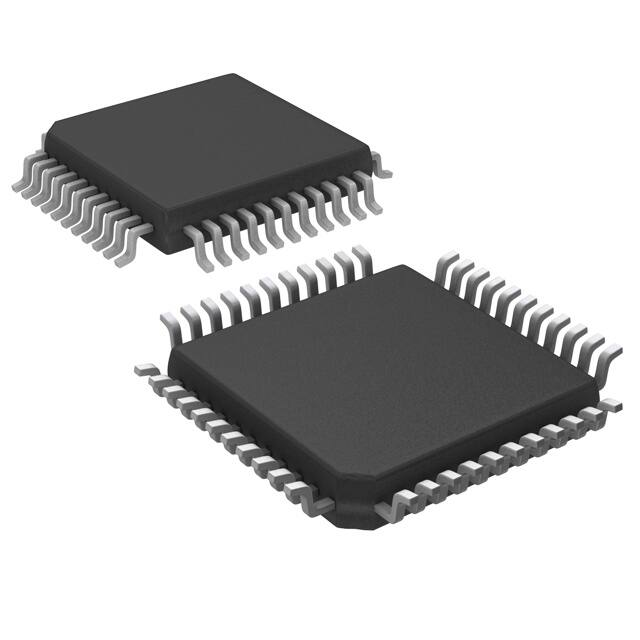
The SCOUT is a CMOS device offered in a P-MQFP-44 package and operates with a
3.3V or 5V supply.
Data Sheet
1
2001-03-07
�PSB 21391
PSB 21393
Overview
Comparison of the SCOUT with the two chip solution SmartLink -P and
ARCOFI-BA; -SP
SCOUT
SmartLink -P / ARCOFI
Operating modes
TE
TE, TR, HDLC Cont.
Supply voltage
3.3V ± 5 % or 5V ± 5 %
5V ± 5 %
Technology
CMOS
CMOS, BICMOS
Package
P-MQFP-44
P-DSO-28 / P-DSO-28
Transformer ratio for
receiver and transmitter
1:1 (3.3V) or
2:1 (5V)
2:1 (5V)
Transceiver Output Driver
Slower slew rate compared
with SmartLink by slowed
down output drivers
Test loops
Test loop2, 3
Test loop2, 3
Microcontroller Interface
Serial (SCI)
Serial (SCI)
Microcontroller clock
Provided
Provided
( 7.68, 3.84, 0.96MHz,
( 7.68, 3.84, 1,92, 0.96MHz)
disabled or
15.36, 7.68, 1.92 MHz,
disabled if double clock rate
selected)
Register address space
256 byte (32 byte FIFO, 96 4 controlreg., 2 statusreg., 4
byte configuration, 128 byte byte FIFO /
CRAM
12 byte configuration, 128
byte CRAM
Codec CRAM access
(128 byte)
Indirect and direct
addressing (general
purpose RAM)
Indirect addressing
Command structure of the
register access
Header/
address(command)/data
SmartLink specific full
duplex structure
Controller data access to
IOM-2 timeslots
All timeslots; various
possibilities of data access
Not provided
Data control and
manipulation
Various possibilities of data B-channel mute and loop
back
control and data
manipulation (enable/
disable, shifting, looping,
switching)
Transceiver
Data Sheet
2
2001-03-07
�PSB 21391
PSB 21393
Overview
SCOUT
SmartLink -P / ARCOFI
IOM-2
IOM-2 Interface
Double clock (DCL),
Double clock (DCL),
bit clock (BCL),
bit clock pin (BCL),
serial data strobe 1 (SDS1) serial data strobe (SDS)
serial data strobe 2 (SDS2/
RSTO)
Monitor channel
programming
Provided
(MON0 or 1 or 2)
Not provided
C/I channels
CI0 (4bit),
CI1 (4/6bit)
CI0 (4bit),
CI1 (Status of 3bit)
Layer 1 state machine
Equivalent to SmartLink
State machine in software
Possible
Not possible
IDSL (144kBit/s)
Provided (HDLC, SDS)
Not provided
HDLC support
D- and B- channels;
D- channel protocol
Non-auto mode,
transparent mode 0-2,
extended transparent mode
FIFO size
64 bytes per direction with
programmable FIFO
thresholds
2x4 bytes per direction
Undervoltage detection
Provided
Provided
Reset Sources
RST Input
VDDDET
Watchdog
C/I Code Change
EAW Pin
Software Reset
RST Input
VDDDET
Watchdog
Pulse width output LCD
contrast
Not provided
Provided
Codec
Analog inputs
1 single ended, 2 differential 1 single ended, 2 differential
Band gap reference
Externally buffered
Internally buffered
Max. AFE gain transmit
(guaranteed transmission
characteristics)
36 dB differential inputs
24 dB single ended input
42 dB differential inputs
24 dB single ended input
Analog gain steps earpiece
3 dB
6 dB
Data Sheet
3
2001-03-07
�PSB 21391
PSB 21393
Overview
SCOUT
SmartLink -P / ARCOFI
Status indication
Register status bits
Piezo pins
AGC initialization
Initial value
Maximum gain
Voice data manipulation
Three party conferencing
(adding receive and
transmit data)
Voice monitoring on IOM-2
Three party conferencing
(adding receive data)
A-/µ-Law, 8 or 16 bit linear
A-/µ-Law, 16 bit linear
Speakerphone
Voice data formats
Voice monitoring on piezo
output
Mask register for voice data Provided
Not provided
Tone Generator Output
Loudspeaker, earpiece,
piezo pins
Loudspeaker, earpiece
Direct tone generator output Provided
Provided
to loudspeaker
Tone generator signal is
attenuated by -6dB
compared to the ARCOFI;
extended gain range (-24.5,
-27.5dB) in the loudspeaker
amplifier control setting
Saturation amplification of
tone filter, i.e. CRAM
Parameter GE
Data Sheet
As specified
Adjusted to fix value
4
2001-03-07
�PSB 21391
PSB 21393
Siemens Codec with UPNTransceiver
SCOUT-P, SCOUT-PX
Version 1.3
1.1
CMOS
Features
• Serial control interface (SCI)
• IOM-2 interface in TE mode, single/double clock,
two serial data strobe signals
• Various possibilities of microcontroller data access,
data control and data manipulation to all IOM-2
timeslots
• Power supply 3.3 V or 5 V
• Monitor channel handler (master/slave)
•
•
•
•
P-MQFP-44-1
Sophisticated power management for restricted power mode
Programmable microcontroller clock output and reset (input/output) pins
Undervoltage detection and power-on reset generation
Advanced CMOS technology
Transceiver part
• Two wire UPN transceiver with 2B+D channels in half-bauded AMI coding. Fully
compatible to UP0 but for reduced loop length
• Conversion of the frame structure between the UPN interface and IOM-2
• Receive timing recovery
• Continuously adapted receive thresholds
• Activation and deactivation procedures with automatic activation from power down
state
• HDLC controller. Operating in non-auto mode, transparent mode 0-2 or extended
transparent mode. Access to B1, B2 or D channels or the combination of them e.g.
for 144 kbit/s data transmission (2B+D)
Type
Package
PSB 21391
SCOUT-P
P-MQFP-44-1
PSB 21393
SCOUT-PX
P-MQFP-44-1
Data Sheet
5
2001-03-07
�PSB 21391
PSB 21393
Overview
• FIFO buffer with 64 bytes per direction and programmable FIFO thresholds for
efficient transfer of data packets
• D-channel access control
• Implementation of IOM-2 MONITOR and C/I-channel protocol to control peripheral
devices
• Realization of layer 1 state machine in software possible
• Watchdog timer
• Programmable reset sources
• Test loops and functions
Codec part
•
•
•
•
•
•
•
•
•
•
•
•
•
•
•
Applications in digital terminal equipment featuring voice functions
Digital signal processing performs all CODEC functions
Fully compatible with the ITU-T G.712 and ETSI (NET33) specification
PCM A-Law/µ-Law (ITU-T G.711) and 8/16-bit linear data; maskable codec data
Flexible configuration of all internal functions
Three analog inputs for the handset microphone, the speakerphone and the headset
Two differential outputs for a handset earpiece (200 Ω) and a loudspeaker (50 Ω for
5V power supply, 25 Ω for 3.3V power supply)
Flexible test and maintenance loopbacks in the analog front end and the digital signal
processor
Independent gain programmable amplifiers for all analog inputs and outputs
Full digital speakerphone (SCOUT-PX PSB 21393 only) and loudhearing support
without any external components (speakerphone test and optimization function is
available)
Enhanced voice data manipulation for features like:
- Three-party conferencing
- Voice monitoring
Two transducer correction filters
Side tone gain adjustment
Flexible DTMF, tone and ringing generator
Direct and indirect CRAM access
Data Sheet
6
2001-03-07
�PSB 21391
PSB 21393
Overview
BCL
FSC
DCL
V SSPLL
V DDPLL
reserved
reserved
V SSL
V DDL
LIa
Pin Configuration
LIb
1.2
33 32 31 30 29 28 27 26 25 24 23
VDDSEL
34
22
DU
VDDDET
35
21
DD
VDDA
36
20
SDX
VSSA
37
19
SDR
VREF
38
18
SCLK
BGREF
39
17
VSSD
AXI
40
16
VDDD
MIN2
41
15
EAW
MIP2
42
14
XTAL1
MIN1
43
13
XTAL2
MIP1
44
12
MCLK
1
2
3
4
5
6
7
8
9 10 11
V DDP
LSP
V SSP
LSN
HOP
HON
CS
INT
RST
RSTO/SDS2
SDS1
SCOUT-P(X)
PSB 21391
(PSB 21393)
P-MQFP-44
mqfp44_pin_upn.vsd
Figure 1
Pin Configuration
Data Sheet
7
2001-03-07
�PSB 21391
PSB 21393
Overview
1.3
Logic Symbol
IOM-2 Interface
5
VDD
5
VSS VDDSEL DD
VREF
BGREF
DU FSC DCL BCL SDS1 RSTO/
SDS2
Analog Front End
RST
AXI
VDDDET
MIP1
MIN1
LIa
MIP2
LIb
MIN2
XTAL2
HOP
HON
XTAL1
UPN Interface
15.36 MHz
EAW
LSP
LSN
CS
INT MCLK SCLK SDR SDX
Serial Control Interface (SCI)
VDD:
5 separate power pins
(VDDL,VDDD,VDDA,VDDP,VDDPLL)
VSS:
5 separate ground pins
(VSSL,VSSD,VSSA,VSSP,VSSPLL)
logsym_upn.vsd
Figure 2
Logic Symbol of the SCOUT in P-MQFP-44
Data Sheet
8
2001-03-07
�PSB 21391
PSB 21393
Overview
1.4
Pin Definitions and Function
Table 1
Pin No. Symbol
Input (I)
Output (O)
Open Drain
(OD)
Function
Power supply (3.3 V or 5 V ± 5 %)
26
VDDL
VDDD
VDDA
VDDP
VDDPLL
VSSL
VSSD
VSSA
VSSP
VSSPLL
–
Ground for internal PLL
34
VDDSEL I
VDD Selection
’0’: 3.3 V supply voltage
’1’: 5 V supply voltage
31
16
36
1
27
30
17
37
3
–
Supply voltage for line driver
–
Supply voltage for digital parts
–
Supply voltage for analog parts
–
Supply voltage for loudspeaker
–
Supply voltage for internal PLL
–
Ground for line driver
–
Ground for digital parts
–
Ground for analog parts
–
Ground for loudspeaker
IOM-2 Interface
21
DD
I/OD/O
Data Downstream
22
DU
I/OD/O
Data Upstream
25
FSC
I/O
Frame Synchronization Clock (8 kHz)
24
DCL
I/O
Data Clock (double clock, 1.536 MHz)
23
BCL
O
Bit Clock (768kHz)
11
SDS1
O
Programmable strobe signal or bit clock
10
RSTO/
SDS2
OD
O
Reset Output (active low)
Strobe signal for each IOM® time slot and/or
D channel indication (programmable)
RESET
9
RST
35
VDDDET I
Data Sheet
I
Reset (active low)
VDD Detection enable (active low)
9
2001-03-07
�PSB 21391
PSB 21393
Overview
Table 1
Pin No. Symbol
Input (I)
Output (O)
Open Drain
(OD)
Function
Transceiver
32
33
LIa
LIb
I/O
I/O
UPN transceiver Line Interface
13
14
XTAL2
XTAL1
OI
I
Oscillator output
Oscillator or 15.36 MHz input
15
EAW
I
External Awake.
A low level on this input starts the oscillator
from the power down state and generates a
reset pulse if enabled (see chapter 7.1.10)
In addition an interrupt request is generated
at pin INT.
Microcontroller Interface
7
CS
I
Chip Select (active low)
8
INT
OD
Interrupt request (active low)
12
MCLK
O
Microcontroller Clock
18
SCLK
I
Clock for the serial control interface
19
SDR
I
Serial Data Receive
20
SDX
OD/O
Serial Data Transmit
Data Sheet
10
2001-03-07
�PSB 21391
PSB 21393
Overview
Table 1
Pin No. Symbol
Input (I)
Output (O)
Open Drain
(OD)
Function
Analog Frontend
38
VREF
O
2.4V Reference voltage for biasing external
circuitry.
An external capacity of ≥ 100nF has to be
connected.
39
BGREF
I/O
Reference Bandgap voltage for internal
references.
An external capacity of ≥ 22nF has to be
connected.
40
AXI
I
Single-ended Auxiliary Input
44
43
MIP1
MIN1
I
I
Symmetrical differential Microphone Input 1
42
41
MIP2
MIN2
I
I
Symmetrical differential Microphone Input 2
5
6
HOP
HON
O
O
Differential Handset earpiece output for
200 Ω transducers
2
4
LSP
LSN
O
O
Differential Loudspeaker output for 50 Ω or
25 Ω loudspeaker using a power supply of
5 V or 3.3 V respectively
Reserved Pins
28
reserved
I
This input is not used for normal operation
and must be connected to VDD.
29
reserved
I
This input is not used for normal operation
and must be connected to VSS.
Data Sheet
11
2001-03-07
�PSB 21391
PSB 21393
Overview
1.5
Typical Applications
The SCOUT can be used in a variety of applications like
•
•
•
•
•
•
PBX voice terminal (Figure 3)
PBX voice terminal with speakerphone (Figure 4)
PBX voice terminal as featurephone with acoustic echo cancellation (Figure 5)
PBX voice terminal with tip/ring extension (Figure 6)
UPN-terminal repeater (Figure 7)
UPN-terminal with S/T-interface option (Figure 8)
SCOUT-P
UPN Interface
SCI
µC
pbx_voice_upn.vsd
Figure 3
PBX Voice Terminal
Data Sheet
12
2001-03-07
�PSB 21391
PSB 21393
Overview
UPN Interface
SCOUT-PX
SCI
µC
voice_te_upn.vsd
Figure 4
PBX Voice Terminal with Speakerphone
UPN Interface
SCOUT-P
IOM-2
SCI
µC
ACE
vt_ace_upn.vsd
Figure 5
PBX Voice Terminal as Featurephone with Acoustic Echo Cancellation
Data Sheet
13
2001-03-07
�PSB 21391
PSB 21393
Overview
UPN Interface
SCOUT-PX
IOM-2
SLIC
SCI
µC
ARCOFI-BA
Fax
vt_tipring_upn.vsd
Figure 6
PBX Voice Terminal with Tip/Ring Extension
UPN Interface
SCOUT-PX
IOM-2
SCI
SmartLink-P
PSB 2197
µC
TR-Mode
UPN Terminal 2
UPN Terminal 1
upn_rep_te_upn.vsd
Figure 7
UPN-Terminal Repeater
Data Sheet
14
2001-03-07
�PSB 21391
PSB 21393
Overview
UPN Interface
SCOUT-PX
IOM-2
S/T Interface
SCI
SBCX
µC
PEB 2081
upn_te_st_upn.vsd
Figure 8
UPN-Terminal with S/T- Interface Option
Data Sheet
15
2001-03-07
�PSB 21391
PSB 21393
Overview
1.6
General Functions and Device Architecture
Figure 9 shows the architecture of the SCOUT containing the following functional
blocks:
• UPN interface transceiver with SmartLink PSB 2197 or ISAC-P TE PSB 2196
functionality respectively
• Serial microcontroller interface
• HDLC controller with 64 byte FlFOs per direction and programmable FIFO threshold
• IOM-2 handler and interface for terminal application, MONITOR handler
• Clock and timing generation
• Digital PLL to synchronize IOM-2 to UPN
• Reset generation (watchdog timer, under voltage detection)
• Analog Front End (AFE) of the codec part
• Digital Signal Processor (DSP) for codec/filter functions, tone generation, voice data
manipulation and speakerphone function (SCOUT-PX)
These functional blocks are described in the following chapters.
Data Sheet
16
2001-03-07
�PSB 21391
PSB 21393
Overview
VR E F
BGR E F
AXI
MIP1
MIN1
MIP2
MIN2
VR E F
AINMUX
AMI
A/D
D/A
Dec
Int
Dec
Int
L P-F ilter
F requency
Correction
F ilter
Digital Gain
Adjus tment
S peakerphone
F unction
T one Generator
Codec
Data
IOM-2 Handler
IOM-2 Interface
DD
HDLC HDLC
L APD
T rans - R ecei- Controller
S tatus
mitter
ver
Command
R egis ter
F IF O
X-F IF O R -F IF O Controller
HDLCData
FSC
MUX
Microcontroller Interface
C/I
MONIT OR
Handler
R es et
MCLK
Interrupt
VDDDE T
S -Data
C/I-Data
T rans c.
Control /
Config.
- T rans ceiver
PN
DPLL
Generation
OS C
LIa
L Ib
XT AL1
XT AL 2
2001-03-07
17
Data Sheet
Controller D ata Acces s
S CI
VD DS E L
T IC B us
Data
T IC
DU
H DL C
Control
C/I D ata
C/I D ata
E AW
S idetone
Codec Control / Config.
DS P
IN T
U
VDD x
VS S x
Monitor Data
VDD DE T
H DL C
D ata
Monitor
Data
MCL K
ALS
AHO
AF E
RST
B CL
S DS 1
S DS 2
S DX
S DR
S CL K
T IC B us Data
RSTO
D CL
CS
LS P
LS N
HOP
HON
AR CHIT -U.VS D
D ata S ource S election, Voice Data Manipulation
(Coding, Mas king, Conferencing)
Figure 9
Architecture of the SCOUT
�PSB 21391
PSB 21393
Interfaces
2
Interfaces
The SCOUT provides the following interfaces:
• Serial microcontroller interface together with a reset and microcontroller clock
generation.
• IOM-2 interface as an universal backplane for terminals
• UPN interface towards the two wire subscriber line
• Analog Front End (AFE) as interface between the analog transducers and the digital
signal processor of the codec part
The microcontroller and IOM-2 interface are described in chapter 2.1 or 2.2
respectively. The UPN interface is described in the chapter 2.3, the analog front end
(AFE) in chapter 4.1
Data Sheet
18
2001-03-07
�PSB 21391
PSB 21393
Interfaces
2.1
Microcontroller Interface
The SCOUT supports a serial microcontroller interface. For applications where no
controller is connected to the SCOUT microcontroller interface programming is done via
the IOM-2 MONITOR channel from a master device. In such applications the SCOUT
operates in the IOM-2 slave mode (refer to the corresponding chapter of the IOM-2
MONITOR handler).
The interface selections are all done by pinstrapping. The possible interface selections
are listed in table 2. The selection pins are evaluated when the reset input RST or a reset
of the undervoltage detection is released. For the pin levels stated in the tables the
following is defined:
’High’:
dynamic pin value which must be ’High’ when the pin level is evaluated
VDD, VSS: static ’High’ or ’Low’ level
Table 2
Interface Selection
PIN
CS
Interface
Type/Mode
‘High’
Serial Control Interface
(SCI)
VSS
IOM-2 MONITOR Channel
(Slave Mode)
The mapping of all accessible registers can be found in figure 82 in chapter 7.
The microcontroller interface also consists of a microcontroller clock generation at pin
MCLK and an interrupt request at pin INT.
Data Sheet
19
2001-03-07
�PSB 21391
PSB 21393
Interfaces
2.1.1
Serial Control Interface (SCI)
The serial control interface (SCI) is compatible to the SPI interface of Motorola or
Siemens C510 family of microcontrollers.
The SCI consists of 4 lines: SCLK, SDX, SDR and CS. Data are transferred via the lines
SDR and SDX at the rate given by SCLK. The falling edge of CS indicates the beginning
of a serial access to the registers. Incoming data is latched at the rising edge of SCLK
and shifts out at the falling edge of SCLK. Each access must be terminated by a rising
edge of CS. Data is transferred in groups of 8 bits with the MSB first.
Figure 10 shows the timing of a one byte read/write access via the serial control
interface.
Data Sheet
20
2001-03-07
�PSB 21391
PSB 21393
Interfaces
Figure 10
Serial Control Interface Timing
Data Sheet
21
2001-03-07
�PSB 21391
PSB 21393
Interfaces
2.1.1.1
Programming Sequences
The principle structure of a read/write access to the SCOUT registers via the serial
control interface is shown in figure 11.
write sequence:
write
byte 2
header
SDR
7
0
0 7
read sequence:
byte 3
address (command)
6
write data
0
7
0
7
0
read
byte 2
header
SDR
7
1
0 7
address (command)
6
SDX
byte 3
0
read data
Figure 11
Serial Command Structure
A new programming sequence starts with the transfer of a header byte. The header byte
specifies different programming sequences allowing a flexible and optimized access to
the individual functional blocks of the SCOUT.
The possible sequences are listed in table 3 and are described afterwards.
Table 3
Header Byte Code
Header
Byte
Sequence Type
Access to
00H
Cmd-Data-Data-Data ARCOFI compatible,
non-interleaved
Codec reg./CRAM
(indirect)
08H
ARCOFI compatible,
interleaved
40H
non-interleaved
44H
48H
Sequence
Adr-Data-Adr-Data
CRAM (80H-FFH)
interleaved
4CH
Data Sheet
Address Range 00H-6FH
Address Range 00H-6FH
CRAM (80H-FFH)
22
2001-03-07
�PSB 21391
PSB 21393
Interfaces
Table 3
Header Byte Code
4AH
Read-/Write-only
4EH
(address autoincrement) CRAM (80H-FFH)
Adr-Data-Data-Data
43H
Address Range 00H-6FH
Read-/Write-only
41H
non-interleaved
49H
interleaved
Address Range 00H-6FH
Header 00H: ARCOFI Compatible Sequence
This programming sequence is compatible to the SOP, COP and XOP command
sequences of the ARCOFI. It gives indirect access to the codec registers 60H-6FH and
the CRAM (80H-FFH). The codec command word (cmdw) is followed by a defined
number of data bytes (data n; n = 0, 1, 4 or 8). The number of data bytes depends on the
codec command word. The commands can be applied in any order and number. The
coding of the different SOP, COP and XOP commands is listed in the description of the
command word (CMDW) in chapter 4.8.
Structure of the ARCOFI compatible sequence:
defined length
defined length
00H
cmdw
data n
data 1
cmd
data n
data 1
Header 40H, 44H: Non-interleaved A-D-A-D Sequences
The non-interleaved A-D-A-D sequences give direct read/write access to the address
range 00H-6FH (header 40H) or the CRAM range 80H-FFH (header 44H) respectively and
can have any length. In this mode SDX and SDR can be connected together allowing
data transmission on one line.
Example for a read/write access with header 40H or 44H:
SDR
header
SDX
Data Sheet
wradr
wrdata
rdadr
rdadr
rddata
23
wradr
wrdata
rdata
2001-03-07
�PSB 21391
PSB 21393
Interfaces
Header 48H, 4CH: Interleaved A-D-A-D Sequences
The interleaved A-D-A-D sequences give direct read/write access to the address range
00H-6FH (header 48H) or the CRAM range 80H-FFH (header 4CH) respectively and can
have any length. This mode allows a time optimized access to the registers by
interleaving the data on SDX and SDR.
Example for a read/write access with header 48H or 4CH:
SDR
header
wradr
wrdata
rdadr
SDX
rdadr
wradr
rddata
rddata
wrdata
Header 4AH, 4EH: Read-/Write-only A-D-D-D Sequences (Address Auto increment)
The A-D-D-D sequences give a fast read-/write-only access to the address range 00H6FH (header 4AH) or the CRAM range 80H-FFH (header 4EH) respectively.
The starting address (wradr, rdadr) is incremented automatically after every data byte.
The sequence can have any length and is terminated by the rising edge of CS.
Example for a write access with header 4AH or 4EH:
SDR
header
wradr
wrdata
wrdata
wrdata
wrdata
wrdata
wrdata
wrdata
(wradr)
(wradr+1)
(wradr+2)
(wradr+3)
(wradr+4)
(wradr+5)
(wradr+6)
SDX
Example for a read access with header 4AH or 4EH:
SDR
header
SDX
Data Sheet
rdadr
rddata
rddata
rddata
rddata
rddata
rddata
rddata
(rdadr)
(rdadr+1)
(rdadr+2)
(rdadr+3)
(rdadr+4)
(rdadr+5)
(rdadr+6)
24
2001-03-07
�PSB 21391
PSB 21393
Interfaces
Header 43H: Read-/Write- only A-D-D-D Sequence
This mode (header 43H) can be used for a fast access to the HDLC FIFO data. Any
address (rdadr, wradr) in the range between 00h and 1F gives access to the current
FIFO location selected by an internal pointer which is automatically incremented with
every data byte following the first address byte. The sequence can have any length and
is terminated by the rising edge of CS.
Example for a write access with header 43H:
SDR
header
wradr
wrdata
wrdata
wrdata
wrdata
wrdata
wrdata
wrdata
(wradr)
(wradr)
(wradr)
(wradr)
(wradr)
(wradr)
(wradr)
SDX
Example for a read access with header 43H:
SDR
header
rdadr
SDX
rddata
rddata
rddata
rddata
rddata
rddata
rddata
(rdadr)
(rdadr)
(rdadr)
(rdadr)
(rdadr)
(rdadr)
(rdadr)
Header 41H: Non-interleaved A-D-D-D Sequence
This sequence (header 41H) allows in front of the A-D-D-D write access a noninterleaved A-D-A-D read access. This mode is useful for reading status information
before writing to the HDLC XFIFO. The termination condition of the read access is the
reception of the wradr. The sequence can have any length and is terminated by the rising
edge of CS.
Example for a read/write access with header 41H:
SDR
header
rdadr
SDX
rdadr
rddata
wradr
wrdata
wrdata
wrdata
(wradr)
(wradr)
(wradr)
rddata
Header 49H: Interleaved A-D-D-D Sequence
This sequence (header 49H) allows in front of the A-D-D-D write access an interleaved
A-D-A-D read access. This mode is useful for reading status information before writing
to the HDLC XFIFO. The termination condition of the read access is the reception of the
wradr. The sequence can have any length and is terminated by the rising edge of the CS
line.
Example for a read/write access with header 49H:
SDR
header
SDX
Data Sheet
rdadr
rdadr
rddata
wradr
wrdata
wrdata
wrdata
(wradr)
(wradr)
(wradr)
rddata
25
2001-03-07
�PSB 21391
PSB 21393
Interfaces
2.1.2
Interrupt Structure and Logic
Special events in the SCOUT are indicated by means of a single interrupt output, which
requests the host to read status information from the SCOUT or transfer data from/to the
SCOUT.
Since only one INT request output is provided, the cause of an interrupt must be
determined by the host reading the interrupt status registers of the SCOUT.
The structure of the interrupt status registers is shown in figure 12.
MSTI
STOV21
STOV20
STOV11
STOV10
STI21
STI20
STI11
STI10
MASK
ISTA
ST
CIC
TIN
WOV
TRAN
MOS
HDLC
ST
CIC
TIN
WOV
TRAN
MOS
HDLC
INT
STI
STOV21
STOV20
STOV11
STOV10
STI21
STI20
STI11
STI10
ASTI
ACK21
ACK20
ACK11
ACK10
CIC0
CIC1
CIR0
CI1E
CIX1
RME
RPF
RFO
XPR
RME
RPF
RFO
XPR
XMR
XDU
XMR
XDU
MASKH
ISTAH
MASKTR
LD
RIC
ISTATR
LD
RIC
MRE
MDR
MER
MIE
MDA
MAB
MOSR
MOCR
Figure 12
SCOUT Interrupt Status Registers
Data Sheet
26
2001-03-07
�PSB 21391
PSB 21393
Interfaces
Five interrupt bits in the ISTA register point at interrupt sources in the HDLC Controller
(HDLC), Monitor- (MOS) and C/I- (CIC) handler, the transceiver (TRAN) and the
synchronous transfer (ST). The timer interrupt (TIN) and the watchdog timer overflow
(WOV) can be read directly from the ISTA register. All these interrupt sources are
described in the corresponding chapters. After the SCOUT has requested an interrupt
by setting its INT pin to low, the host must read first the SCOUT interrupt status register
(ISTA) in the associated interrupt service routine. The INT pin of the SCOUT remains
active until all interrupt sources are cleared by reading the corresponding interrupt
register. Therefore it is possible that the INT pin is still active when the interrupt service
routine is finished.
Each interrupt indication of the interrupt status registers can selectively be masked by
setting the respective bit in the MASK register.
For some interrupt controllers or hosts it might be necessary to generate a new edge on
the interrupt line to recognize pending interrupts. This can be done by masking all
interrupts at the end of the interrupt service routine (writing FFH into the MASK register)
and write back the old mask to the MASK register.
A low level at pin EAW generates an interrupt indication which is set at the LD bit of the
ISTATR register. If this LD bit has been set due to an level detect interrupt, the LD bit in
the transceiver status register TR_STA is set additionally.
Therefore pin EAW has to be connected to ’1’, if no interrupt should be generated.
Data Sheet
27
2001-03-07
�PSB 21391
PSB 21393
Interfaces
2.1.3
Microcontroller Clock Generation
The microcontroller clock is provided by the pin MCLK. Five clock rates are selectable by
a programmable prescaler (see chapter clock generation figure 78) which is controlled
by the MODE1.MCLK bit corresponding following table. By setting the clock divider
selection bit (MODE1.CDS) a doubled MCLK frequency is available.
The possible MCLK frequencies are listed in table 4.
Table 4
MCLK Frequencies
MCLK
Bits
MCLK Frequency
with MODE1.CDS = ’0’
MCLK Frequency
with MODE1.CDS = ’1’
’00’
3.84 MHz (default)
7.68 MHz (default)
’01’
0.96 MHz
1.92 MHz
’10’
7.68 MHz
15.36 MHz
’11’
disabled
disabled
The clock rate is changed after CS becomes inactive.
Data Sheet
28
2001-03-07
�PSB 21391
PSB 21393
Interfaces
2.2
IOM-2 Interface
The SCOUT supports the IOM-2 interface in terminal mode with single clock and double
clock. The IOM-2 interface consists of four lines: FSC, DCL, DD and DU. The rising edge
of FSC indicates the start of an IOM-2 frame. The FSC signal is generated by the receive
DPLL which synchronizes to the received line frame. The DCL and the BCL output clock
signals synchronize the data transfer on both data lines. The DCL is twice the bit rate,
the BCL output rate is equal to the bit rate. The bits are shifted out with the rising edge
of the first DCL clock cycle and sampled at the falling edge of the second clock cycle.
The BCL clock together with the two serial data strobe signals (SDS1, SDS2) can be
used to connect time slot oriented standard devices to the IOM-2 interface.
The IOM-2 interface can be enabled/disabled with the DIS_IOM bit in the IOM_CR
register. The BCL clock output can be enabled separately with the EN_BCL bit.
The clock rate or frequency respectively of the IOM-signals in TE mode are:
DD, DU: 768 kbit/s
DCL: 1536 kHz (double clock rate); 768 kHz (single clock rate if DIS_TR = ’1’)
FSC: 8 kHz.
If the transceiver is disabled (TR_CONF.DIS_TR) the DCL and FSC pins become input
and the HDLC and codec parts can still work via IOM-2. In this case it can be selected
with the clock mode bit (IOM_CR.CLKM) between a double clock and a single clock
input.
Note: One IOM-2 frame has to consist of a multiple of 64 (32) DCL clocks for a double
(single) clock selection.
FSC
DCL
BCL
Figure 13 Clock waveforms
Data Sheet
29
2001-03-07
�PSB 21391
PSB 21393
Interfaces
2.2.1
IOM-2 Frame Structure
The frame structure on the IOM-2 data ports (DU,DD) in IOM-2 terminal mode is shown
in figure 14 .
Figure 14
IOM-2 Frame Structure in Terminal Mode
The frame is composed of three channels
• Channel 0 contains 144-kbit/s of user and signaling data (2B + D), a MONITOR
programming channel (MON0) and a command/indication channel (CI0) for control
and programming of the layer-1 transceiver.
• Channel 1 contains two 64-kbit/s intercommunication channels (IC) plus a MONITOR
and command/indicate channel (MON1, CI1) to program or transfer data to other IOM2 devices.
• Channel 2 is used for the TlC-bus access. Additionally channel 2 supports further IC
and MON channels.
Note: Each octet related to any integrated functional block can be programmed to any
timeslot (see chapter 7.2.2) except the C/I0- and D- channels that are always
related to timeslot 0.
Data Sheet
30
2001-03-07
�PSB 21391
PSB 21393
Interfaces
2.2.2
IOM-2 Handler
The IOM-2 handler offers a great flexibility for handling the data transfer between the
different functional units of the SCOUT and voice/data devices connected to the IOM-2
interface. Additionally it provides a microcontroller access to all time slots of the IOM-2
interface via the four controller data access registers (CDA). Figure 15 shows the
architecture of the IOM-2 handler. For illustrating the functional description it contains all
configuration and control registers of the IOM-2 handler. A detailed register description
can be found in chapter 7.2
The PCM data of the functional units
• Codec (CO)
• Transceiver (TR) and the
• Controller data access (CDA)
can be configured by programming the time slot and data port selection registers
(TSDP). With the TSS bits (Time Slot Selection) the PCM data of the functional units can
be assigned to each of the 12 PCM time slots of the IOM-2 frame. With the DPS bit (Data
Port Selection) the output of each functional unit is assigned to DU or DD respectively.
The input is assigned vice versa. With the control registers (CR) the access to the data
of the functional units can be controlled by setting the corresponding control bits ( EN,
SWAP).
To avoid data collisions it has to be noticed that the C/I and D channels of the enabled
transceiver are always related to time slot 3. If the monitor handler is enabled its data is
related to time slot TS (2, 6 or 10) and the appropriate MR and MX bits to time slot TS+1
depending on the MCS bits of register MON_CR.
The IOM-2 handler provides also access to the
• MONITOR channel (MON)
• C/I channels (CI0,CI1)
• TIC bus (TIC) and
• D- and B-channel for HDLC control
The access to these channels is controlled by the registers HCI_CR and MON_CR.
The IOM-2 interface with the two Serial Data Strobes (SDS1,2) is controlled by the
control registers IOM_CR, SDS1_CR and SDS2_CR.
The reset configuration of the SCOUT IOM-2 handler corresponds to the defined frame
structure and data ports in IOM-2 terminal mode (see figure 14).
Data Sheet
31
2001-03-07
�32
IOMHAND.VSD
CO10R
CO11R
CO20R
CO21R
CO10X
CO11X
CO20X
CO21X
x,y = 1 or 2
CO_T S DPxy
CO_CR
Control
Codec Data
(T S S , DPS ,
E N)
Codec Data
CDA10
CDA11
CDA20
CDA21
CDA
R egis ter
Controller Data
Acces s (CDA)
DD
DU
CDA Data
CDA_T S DPxy
CDA_CR x
MCDA
STI
MS T I
AS T I
Control
Data Acces s
(T S DP, DPS ,
E N, S WAP,
T BM, MCDA,
S T I)
(E N, OD)
IOM-2 Interface
Handler
MON
MON_CR
T IC
IOM_CR
CI0
(E N, T LE N, T S S )
Data
Control
Monitor T IC Bus
Data
Dis able
(DPS ,E N (T IC_DIS )
MCS )
Monitor Data
Microcontroller Interface
S DS 1/2_CR
IOM_CR
T IC B us Data
IOM-2 Handler
CI0 Data
S DS 1 S DS 2
CI1
HDLC F IF O
HCI_CR
Control
Control
HDL C
C/I1
D-, BData
Data
(DPS ,E N)
(E N)
CI1 Data
Data Sheet
D/B 1/B 2 Data
DU DD F S C DCL B CL
DD
DU
B 1/B 2/D - Data
C/IO - Data
T R _CR
T R _T S DP_B2
T R _T S DP_B1
Control
T rans ceiver
Data
Acces s
(T S S , DPS ,
E N)
T R _D_R
T R _B 1_R
T R _B 2_R
T R _B1_X
T R _B2_X
T R _D_X
PSB 21391
PSB 21393
Interfaces
.
Figure 15
Architecture of the IOM Handler
2001-03-07
T rans ceiver
Data (T R )
Codec Data (CO)
�PSB 21391
PSB 21393
Interfaces
2.2.2.1
Controller Data Access (CDA)
The IOM-2 handler provides with its four controller data access registers (CDA10,
CDA11, CDA20, CDA21) a very flexible solution for the access to the 12 IOM-2 time slots
by the microcontroller.
The functional unit CDA (controller data access) allows with its control and configuration
registers
• looping of up to four independent PCM channels from DU to DD or vice versa with the
four CDA registers
• shifting or switching of two independent PCM channels to another two independent
PCM channels on both data ports (DU, DD)
• monitoring of up to four time slots on the IOM-2 interface simultaneously
• microcontroller read and write access to each PCM channel
The access principle which is identical for the two channel register pairs CDA10/11 and
CDA20/21 is illustrated in figure 16. The index variables x,y used in the following
description can be 1 or 2 for x, and 0 or 1 for y. The prefix ’CDA_’ from the register names
has been omitted for simplification.
To each of the four CDAxy data registers a CDA_TSDPxy register is assigned by which
the time slot and the data port can be determined. With the TSS (Time Slot Selection)
bits a time slot from 0...11 can be selected. With the DPS (Data Port Selection) bit the
output of the CDAxy register can be assigned to DU or DD respectively. The time slot
and data port for the output of CDAxy is always defined by its own CDA_TSDPxy
register. The input of CDAxy depends on the SWAP bit in the control registers CRx.
If the SWAP bit = ’0’ the time slot and data port for the input and output of the CDAxy
register is defined by its own CDA_TSDPxy register. The data port for the CDAxy input
is vice versa to the output setting for CDAxy.
If the SWAP bit = ’1’, the input port and time slot of the CDAx0 is defined by the
CDA_TSDP register of CDAx1 and the input port and time slot of CDAx1 is defined by
the CDA_TSDP register of CDAx0.
The input and output of every CDAxy register can be enabled or disabled by setting the
corresponding EN (-able) bit in the control register CDAx_CR. If the input of a register is
disabled the output value in the register is retained.
Data Sheet
33
2001-03-07
�PSB 21391
PSB 21393
Interfaces
.
TSa
TSb
DU
Control
Register
CDAx0
0
1
1
Time Slot
Selection (TSS)
Enable
input
output
(EN_I1)
(EN_O1)
Input
Swap
(SWAP)
1
1
1
1
CDAx1
1
1
0
CDA_TSDPx1
1
0
Data Port
Selection (DPS)
Time Slot
Selection (TSS)
Enable
output
input
(EN_O0) (EN_I0)
Data Port
Selection (DPS)
CDA_TSDPx0
CDA_CRx
0
1
DD
TSa
TSb
IOM_HAND.FM4
x = 1 or 2; a,b = 0...11
Figure 16
Data Access via CDAx0 and CDAx1 register pairs
2.2.2.1.1 Looping and Shifting Data
Figure 17 gives examples for typical configurations with the above explained control and
configuration possibilities with the bits TSS, DPS, EN and SWAP in the registers
TSDPxy or CDAx_CR:
a) looping IOM-2 time slot data from DU to DD or vice versa (SWAP = ’0’)
b) shifting data from TSa to TSb on DU and DD (SWAP = ’1’)
c) switching data from TSa (DU) to TSb(DD) and TSb (DU) to TSa (DD)
Data Sheet
34
2001-03-07
�PSB 21391
PSB 21393
Interfaces
a) Looping Data
TSa
TSb
CDAx0
CDAx0
.TSS: TSa
TSb
.DPS ’0’
’1’
.SWAP
’0’
DU
DD
b) Shifting Data
TSa
TSb
DU
CDAx0
CDAx0
DD
.TSS: TSa
.DPS ’0’
.SWAP
TSb
’1’
’1’
c) Switching Data
TSa
TSb
CDAx0
CDAx0
.TSS: TSa
.DPS ’0’
.SWAP
TSb
’0’
DU
DD
.x = 1 or 2
’1’
Figure 17
Examples for Data Access via CDAxy Registers
a) Looping Data
b) Shifting Data
c) Switching Data
Data Sheet
35
2001-03-07
�PSB 21391
PSB 21393
Interfaces
2.2.2.1.2 Monitoring Data
Figure 18 gives an example for monitoring of two IOM-2 time slots each on DU or DD
simultaneously. For monitoring on DU and/or DD the channel registers with even
numbers (CDA10, CDA20) are assigned to time slots with even numbers TS(2n) and the
channel registers with odd numbers (CDA11, CDA21) are assigned to time slots with odd
numbers TS(2m+1) (n,m = 0...5). The user has to take care of this restriction by
programming the appropriate time slots.
.
a) Monitoring Data
EN_O: ’0’
CDA_CR1. EN_I: ’1’
DPS: ’0’
TSS: TS(2n)
’0’
’1’
’0’
TS(2m+1)
DU
CDA10
CDA11
CDA20
CDA21
TSS: TS(2n)
’1’
DPS:
CDA_CR2.
EN_I: ’1’
EN_O: ’0’
TS(2m+1)
’1’
’1’
’0’
DD
n,m = 0...5
Figure 18
Example for Monitoring Data
2.2.2.1.3 Monitoring TIC Bus
Monitoring the TIC bus (TS11) is handled as a special case. The TIC bus can be
monitored with the registers CDAx0 by setting the EN_TBM (Enable TIC Bus Monitoring)
bit in the control registers CRx. The TSDPx0 must be set to 08h for monitoring from DU
or 88h for monitoring from DD respectively.
Data Sheet
36
2001-03-07
�PSB 21391
PSB 21393
Interfaces
2.2.2.1.4 Synchronous Transfer
While looping, shifting and switching (see figure 21 and 22) the data can be accessed by
the controller between the synchronous transfer interrupt (STI) and the synchronous
transfer overflow interrupt (STOV).
The microcontroller access to the CDAxy registers can be synchronized by means of
four programmable synchronous transfer interrupts (STIxy) and synchronous transfer
overflow interrupts (STOVxy) in the STI register.
Depending on the DPS bit in the corresponding CDA_TSDPxy register the STIxy is
generated two (for DPS=’0’) or one (for DPS=’1’) BCL clock after the selected time slot
(CDA_TSDPxy.TSS). One BCL clock is equivalent to two DCL clocks.
A non masked synchronous transfer overflow (STOVx0y0) interrupt is generated if the
appropriate STIx1y1 is not acknowledged in time. The STIx1y1 is acknowledged in time
if bit ACKx1y1 in the ASTI register is set to ’1’ one BCL clock (for DPS=’0’) or zero BCL
clocks (for DPS=’1’) before the time slot which is selected for the appropriate STOVx0y0.
If STIx1y1 and STOVx1y1 are not masked STOVx1y1 is only related to STIx1y1 (see
example a), c) and d) of figure 20).
If STIx1y1 is masked but STOVx1y1 is not masked, STOVx0y0 is related to each enabled
STIxy (see example b) and d) of figure 20).
Setting the corresponding bits in the MSTI (Mask Synchronous Transfer Interrupts)
register masks the STIxy and the STOVxy interrupt. The interrupt structure of the
synchronous transfer is shown in figure 19. Examples of the described synchronous
transfer interrupt controlling are illustrated in Figure 20. A read to the STI register clears
the STIxy and STOVxy interrupts.
.
INT
ST
CIC
TIN
WOV
TRAN
MOS
HDLC
ST
CIC
TIN
WOV
TRAN
MOS
HDLC
MASK
ISTA
STOV21
STOV20
STOV11
STOV10
STI21
STI20
STI11
STI10
MSTI
STOV21
STOV20
STOV11
STOV10
STI21
STI20
STI11
STI10
STI
ACK21
ACK20
ACK11
ACK10
ASTI
Figure 19
Interrupt Structure of the Synchronous Data Transfer
Data Sheet
37
2001-03-07
�PSB 21391
PSB 21393
Interfaces
.
: STI interrupt generated
: STOV interrupt generated for a not acknowledged STI interrupt
a) Interrupts for data access to time slot 0 (B1 after reset), MSTI.STI10 and MSTI.STOV10 enabled
xy:
CDA_TDSPxy.TSS:
MSTI.STIxy:
MSTI.STOVxy:
10
TS0
’0’
’0’
11
TS1
’1’
’1’
TS11 TS0 TS1 TS2 TS3
21
TS5
’1’
’1’
20
TS11
’1’
’1’
TS4 TS5 TS6 TS7 TS8 TS9 TS10 TS11 TS0
b) Interrupts for data access to time slot 0 (B1 after reset), STOV interrupt used as flag for "last possible CDA
access"; MSTI.STI10 and MSTI.STOV20 enabled
xy:
CDA_TDSPxy.TSS:
MSTI.STIxy:
MSTI.STOVxy:
10
TS0
’0’
’1’
11
TS1
’1’
’1’
TS11 TS0 TS1 TS2 TS3
21
TS5
’1’
’1’
20
TS11
’1’
’0’
TS4 TS5 TS6 TS7 TS8 TS9 TS10 TS11 TS0
c) Interrupts for data access to time slot 0 and 1 (B1 and B2 after reset), MSTI.STI10, MSTI.STOV10,
MSTI.STI11 and MSTI.STOV11 enabled
xy:
CDA_TDSPxy.TSS:
MSTI.STIxy:
MSTI.STOVxy:
10
TS0
’0’
’0’
11
TS1
’0’
’0’
TS11 TS0 TS1 TS2 TS3
21
TS5
’1’
’1’
20
TS11
’1’
’1’
TS4 TS5 TS6 TS7 TS8 TS9 TS10 TS11 TS0
d) Interrupts for data access to time slot 0 (B1 after reset), STOV20 interrupt used as flag for "last possible CDA
access", STOV10 interrupt used as flag for "CDA access failed"; MSTI.STI10, MSTI.STOV10 and
MSTI.STOV20 enabled
xy:
CDA_TDSPxy.TSS:
MSTI.STIxy:
MSTI.STOVxy:
10
TS0
’0’
’0’
11
TS1
’1’
’1’
TS11 TS0 TS1 TS2 TS3
21
TS5
’1’
’1’
20
TS11
’1’
’0’
TS4 TS5 TS6 TS7 TS8 TS9 TS10 TS11 TS0
sti_stov.vsd
Figure 20
Examples for the Synchronous Transfer Interrupt Control with one enabled STIxy
Data Sheet
38
2001-03-07
�PSB 21391
PSB 21393
Interfaces
Figure 21 shows the timing of looping TSa on DU to TSa on DD (a = 0...11) via CDAxy
register. TSa is read in the CDAxy register from DU and is written one frame later on DD.
.
a = 0...11
FSC
DU
TSa
TSa
WR
RD
µC
DD
TSa
STOV
*)
STI
ACK
STI
CDAxy
TSa
*) if access by the µC is required
Figure 21
Data Access when Looping TSa from DU to DD
Data Sheet
39
2001-03-07
�PSB 21391
PSB 21393
Interfaces
Figure 22 shows the timing of shifting data from TSa to TSb on DU(DD). In figure 22a)
shifting is done in one frame because TSa and TSb didn’t succeed direct one another
(a,b = 0...9 and b ≥ a+2). In figure 22b) shifting is done from one frame to the following
frame. This is the case when the time slots succeed one other (b = a+1) or b is smaller
than a (b < a).
a) Shifting TSa → TSb within one frame
(a,b: 0...11 and b ≥ a+2)
FSC
DU
(DD)
TSa
TSb
TSa
µC
ACK
*)
STI
STOV
WR
STI
RD
CDAxy
b) Shifting TSa → TSb in the next frame
(a,b: 0...11 and (b = a+1 or b